TSMC’s 2nm chips arriving sooner than expected, by the end of 2025
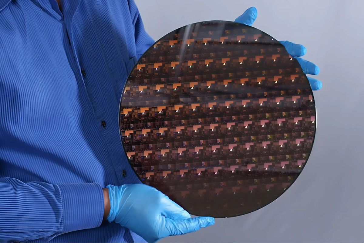
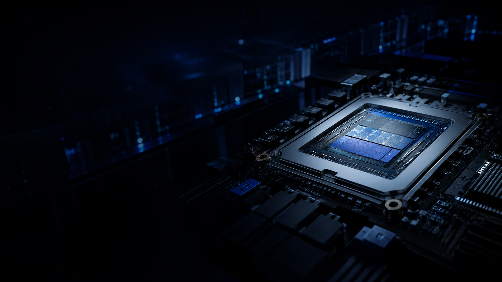
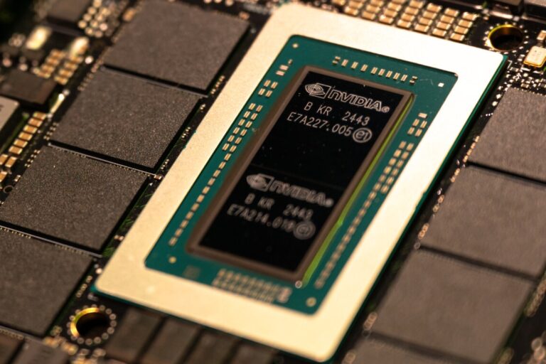
Reports indicate that TSMC is progressing faster than expected in bringing its most advanced chip technology to market. The company has confirmed that its N2 process node will begin volume production before the end of 2025, speeding up both its rollout in Taiwan and its effort to implement the same technology at its Arizona facility.
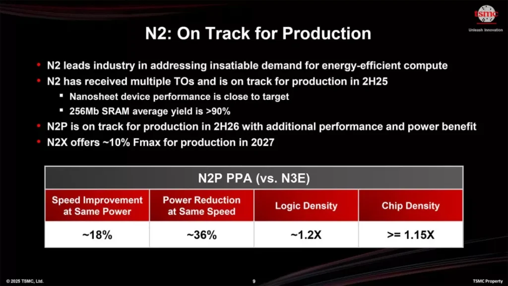
The N2 node introduces nanosheet-based gate-all-around transistors, replacing the FinFET design first used with the 16nm generation. Company executives reported strong initial yields, and large-scale production is expected to expand rapidly through 2026. TSMC is also working on the N2P process, a follow-up scheduled for the second half of 2026, which aims to achieve even greater efficiency improvements.
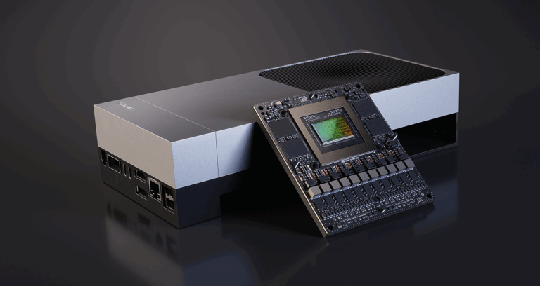
The 2-nanometer breakthrough aligns with record-setting third-quarter financial results. Fueled by growing demand for AI accelerators and premium smartphone chips, TSMC’s revenue surged over 40% year-over-year to $33.1 billion.
Advanced process technologies—including the N3, N5, and N7 families—made up nearly 75% of total sales. Company executives said that capital expenditures will stay high, possibly reaching $42 billion this year, with about three-quarters of that amount focused on expanding cutting-edge manufacturing capacity.
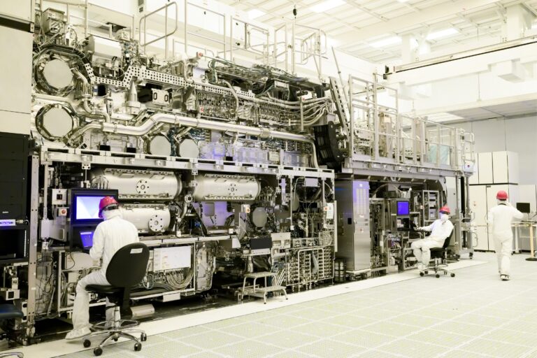
TSMC’s expansion in Arizona now plays a key role in its investment plans. The company has already started producing chips with its N4 process at the first module of Fab 21 near Phoenix, with N3 production expected to follow. During an earnings call this week, CEO C.C. Wei said the company plans to “upgrade our technologies faster to N2 and more advanced processes in Arizona, given the strong AI-related demand from our customers.”
That statement signals a major acceleration, as N2 production at Fab 21 was initially expected to happen by the end of the decade. The simultaneous efforts in Taiwan and the U.S. represent a key stage for the world’s largest contract chipmaker as it works to meet the increasing global demand for high-performance processors used in AI and advanced computing.
Construction of new modules supporting the N2 and its successor, A16, is expected to begin later this year. Once finished, roughly 30% of TSMC’s output from 2-nanometer-class and more advanced process nodes will be produced in the United States.
The Arizona site is expected to become a “GigaFab” complex capable of producing approximately 100,000 wafers per month, with integrated packaging, testing, and local supply chain support.